The inclusion of photonics at a traditional Wafer-Level Packaging...

Photon Capital@PhotonCap
93 views
Mar 03, 2026
~8 min read
Advertisement
1
The inclusion of photonics at a traditional Wafer-Level Packaging symposium (WLPS 2026) highlights a critical industry shift: photonics is now advanced packaging.
The I/O Wall is Real: $NVDA explicitly acknowledging optical interconnects at a packaging event confirms that electrical scaling has hit thermal and bandwidth limits for AI workloads.
Architectural Shifts: The spotlight on Lightmatter’s 3D Photonic Interposer and $INTC's Co-Packaged Optics (CPO) shows the industry is converging on integrating light directly into the compute package.
Scaling for High Volume: $BESI's invited talk on sub-10 µm hybrid bonding proves the ecosystem is aggressively moving from proof-of-concept R&D to resolving yield and mass manufacturing challenges.
I got slide decks and papers, and am thinking of how to share it with you guys in the community here.
smta.org/mpage/wafer-ke…
The I/O Wall is Real: $NVDA explicitly acknowledging optical interconnects at a packaging event confirms that electrical scaling has hit thermal and bandwidth limits for AI workloads.
Architectural Shifts: The spotlight on Lightmatter’s 3D Photonic Interposer and $INTC's Co-Packaged Optics (CPO) shows the industry is converging on integrating light directly into the compute package.
Scaling for High Volume: $BESI's invited talk on sub-10 µm hybrid bonding proves the ecosystem is aggressively moving from proof-of-concept R&D to resolving yield and mass manufacturing challenges.
I got slide decks and papers, and am thinking of how to share it with you guys in the community here.
smta.org/mpage/wafer-ke…
2
$BESI
After verifying that some of Besi SMTA 2026 presentation slides have been already publicly available online, I decided to unpack it. Let's dive into the future of AI Chiplet Packaging, Hybrid Bonding, and CPO.
Along with the rapid growth of AI-related semiconductors, which are seeing a CAGR of 16.5% , the transition to 2.5D/3D systems that combine multiple chiplets is accelerating to overcome the limitations of traditional monolithic structures. To support this shift, Besi has partnered with Applied Materials to establish an integrated Die-to-Wafer (D2W) Hybrid Bonding line.
1. The Ultimate AI Package Architecture
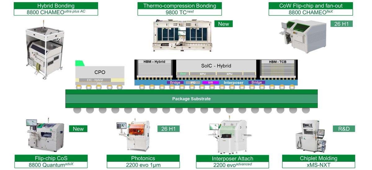
The sheer complexity of next-gen AI architectures is staggering. It’s not just about stacking XPU and HBM anymore; we are seeing the integration of CPO (Co-Packaged Optics) with EIC-PIC Hybrid Bonding and high-precision photonics directly on the same substrate. System-level integration is reaching a whole new level.
2. The Equipment Roadmap
Besi’s equipment roadmap serves as a strong leading indicator for the industry. Both their advanced Hybrid Bonding systems (8800 CHAMEO) and ultra-precise Photonics placement tools (2200 evo 1µm) are targeting 2026 H1. The mass-production cycle for sub-10µm optical and AI packaging is shifting into high gear right now.
3. The "Why" Behind Hybrid Bonding
Why the aggressive push for Hybrid Bonding? The numbers speak for themselves. Compared to a 55µm pitch Si Bridge, moving to a 9µm pitch Hybrid Bonding approach delivers massive gains:
10X Lower Power
10X Lower Added Latency
30X Interconnect Area Reduction
For power-hungry AI and high-speed optics, Cu-Cu direct bonding isn't just an option—it is mandatory.
4. The Scaling Battlefield
TCB (Thermo-compression bonding) is being pushed to its absolute limits, moving towards the 2µm pitch mark. Meanwhile, D2W (Die-to-Wafer) Hybrid Bonding is breaking through into sub-micron territory, driving an exponential increase in 3D interconnect density.
As interconnects scale below 10µm, the synergy between front-end wafer prep and back-end assembly is becoming the ultimate bottleneck.


After verifying that some of Besi SMTA 2026 presentation slides have been already publicly available online, I decided to unpack it. Let's dive into the future of AI Chiplet Packaging, Hybrid Bonding, and CPO.
Along with the rapid growth of AI-related semiconductors, which are seeing a CAGR of 16.5% , the transition to 2.5D/3D systems that combine multiple chiplets is accelerating to overcome the limitations of traditional monolithic structures. To support this shift, Besi has partnered with Applied Materials to establish an integrated Die-to-Wafer (D2W) Hybrid Bonding line.
1. The Ultimate AI Package Architecture
The sheer complexity of next-gen AI architectures is staggering. It’s not just about stacking XPU and HBM anymore; we are seeing the integration of CPO (Co-Packaged Optics) with EIC-PIC Hybrid Bonding and high-precision photonics directly on the same substrate. System-level integration is reaching a whole new level.
2. The Equipment Roadmap
Besi’s equipment roadmap serves as a strong leading indicator for the industry. Both their advanced Hybrid Bonding systems (8800 CHAMEO) and ultra-precise Photonics placement tools (2200 evo 1µm) are targeting 2026 H1. The mass-production cycle for sub-10µm optical and AI packaging is shifting into high gear right now.
3. The "Why" Behind Hybrid Bonding
Why the aggressive push for Hybrid Bonding? The numbers speak for themselves. Compared to a 55µm pitch Si Bridge, moving to a 9µm pitch Hybrid Bonding approach delivers massive gains:
10X Lower Power
10X Lower Added Latency
30X Interconnect Area Reduction
For power-hungry AI and high-speed optics, Cu-Cu direct bonding isn't just an option—it is mandatory.
4. The Scaling Battlefield
TCB (Thermo-compression bonding) is being pushed to its absolute limits, moving towards the 2µm pitch mark. Meanwhile, D2W (Die-to-Wafer) Hybrid Bonding is breaking through into sub-micron territory, driving an exponential increase in 3D interconnect density.
As interconnects scale below 10µm, the synergy between front-end wafer prep and back-end assembly is becoming the ultimate bottleneck.
3
As the semiconductor market pivots toward Heterogeneous Integration, traditional carriers often lead to high yield loss and costly 14–16 week tooling delays.
Gel-Pak’s Universal Carrier (BTXF) solves this by using bio-inspired "Gecko Effect" dry adhesion to securely immobilize dies of any size without custom pockets.
This "pocketless" technology ensures Zero Die Migration for high-speed pick-and-place, significantly boosting OEE and accelerating time-to-market for GenAI and HBM applications.
1. The Yield Paradox in the GenAI Era
The semiconductor market is shifting toward Heterogeneous Integration to meet the massive demand for Generative AI, which is expected to drive 70% of the market by 2030.However, this introduces a "Yield Paradox" where a single faulty chiplet can force the scrapping of an entire high-value package, including costly HBM modules.
2. Defining the Universal Carrier Solution
Gel-Pak’s solution is a pocketless, flexible carrier that adapts to any die size, eliminating the need for custom tooling and reducing time-to-market by up to 16 weeks.Inspired by the "Gecko Effect," it uses bio-inspired dry adhesion to securely immobilize fragile dies while allowing for multiple re-pick cycles.
3. Universal Carrier vs. Conventional MethodsUnlike
JEDEC trays or Tape & Reel, the BTXF carrier offers excellent safety for thin/fragile dies and supports over 250 pick/re-pick cycles. It eliminates tooling costs and potential adhesive residues, providing a clean "drop-in" solution for existing high-volume manufacturing (HVM) tools.
4. Solving Die Migration and Jams
Standard waffle packs carry a high risk of die migration and handler jams, which lead to significant yield loss during automated processes.The micro-textured surface ensures "Zero Die Migration," keeping dies perfectly aligned in a precise grid for high-speed, reliable pick-and-place.


4
$KLAC
Hybrid Bonding, which directly connects copper pads, is emerging as a critical solution for implementing these next-generation packaging structures. However, hybrid bonding reduces interconnect pitches to sub-micron levels (below 10µm), creating a bottleneck that introduces high complexity and extreme defect sensitivity comparable to traditional Front-End processes.
To address these process challenges, this document proposes the implementation of advanced Process Control based on inspection and metrology during the Wafer-to-Wafer (W2W) and Die-to-Wafer (D2W) bonding stages. Since securing Known Good Die (KGD) alone does not guarantee final 3D assembly yield, high-reliability advanced packaging is only possible through the strict control of variables—such as Surface Defectivity, CMP Profile, Die Warpage, and Cu Pad Misalignment—at the nanometer scale.
1. Known Good Die ≠ Known Good 3D Assembly
Demonstrates the mathematical decline of cumulative yield during 3D packaging integration based on individual bonding yields.
The X-axis represents the individual D2D/D2W Bond Yield (90% to 100%), while the Y-axis shows the final 3D Assembly Yield. The curves illustrate that as the number of tiles integrated on a base die increases from 2 to 16, the slope of the final assembly yield drops sharply.
Even if input semiconductors are KGD, the final yield of 3D packaging incorporating multiple chiplets will plummet unless the bonding yield itself is nearly perfect. Therefore, ultra-precise process control over the bonding quality is mandatory.
2. Front End Processes are Blending with Wafer-Level Packaging
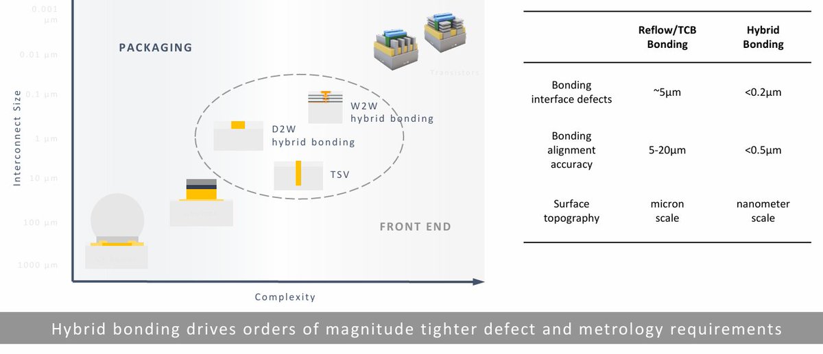
Diagrams the correlation between decreasing interconnect size and increasing process complexity as packaging technology evolves.
It highlights the shift from traditional reflow/TCB bonding to Hybrid Bonding, where interconnect pitches shrink from approximately 10µm to below 1µm. Consequently, requirements for bonding interface defects tighten from ~5µm to <0.2µm, and bonding alignment accuracy tightens from 5–20µm to <0.5µm.
The adoption of hybrid bonding elevates the technical difficulty of packaging to Front-End levels, necessitating metrology and defect management standards that are orders of magnitude more stringent than before
3. 3D Die Stacking Example: Micro Bumping vs. Hybrid Bonding
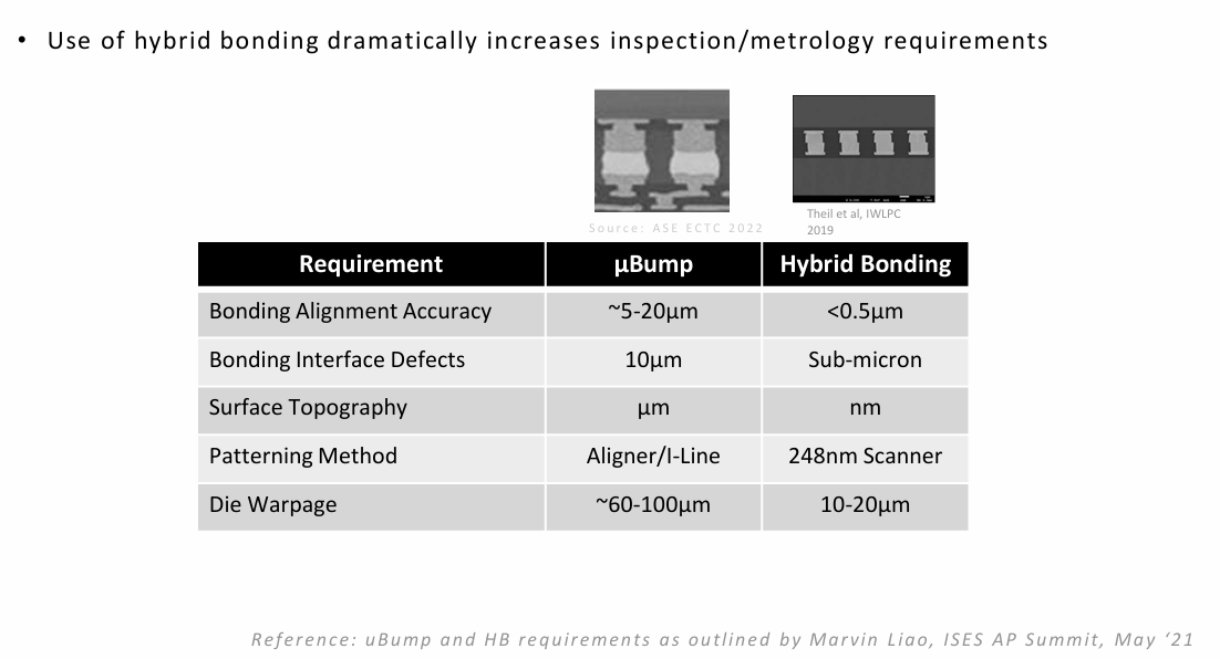
Quantitatively contrasts the requirements for traditional Micro Bumping (μBump) versus cutting-edge Hybrid Bonding.
Technical Details: According to the requirement table, hybrid bonding must control bonding interface defects at a sub-micron level rather than 10µm. Furthermore, Surface Topography must be managed at the nanometer (nm) scale, and Die Warpage must be restricted to 10–20µm.
Because hybrid bonding dramatically narrows process tolerances, the resolution and precision of inspection and metrology equipment must be significantly enhanced to sustain production.
4. Hybrid Bonding: Critical Challenges
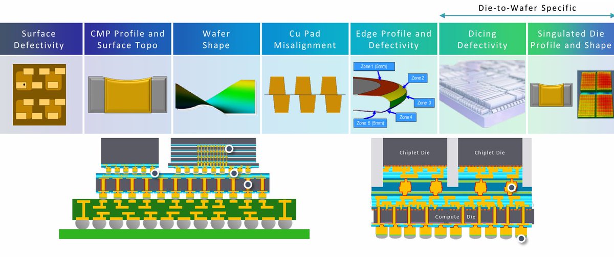
Structures and maps the critical process control challenges encountered during the Die-to-Wafer (D2W) hybrid bonding process.
The interface where the Chiplet Die and Compute Die meet is analyzed across multiple zones. Key control points identified include Surface Defectivity, CMP Profile, Cu Pad Misalignment, and the Singulated Die Profile and Shape (warpage).
Successful mass production of hybrid bonding requires moving beyond simple 2D particle inspection. Investment in multi-faceted metrology infrastructure capable of monitoring 3D die deformation and nano-scale CMP variations is a prerequisite.
Hybrid Bonding, which directly connects copper pads, is emerging as a critical solution for implementing these next-generation packaging structures. However, hybrid bonding reduces interconnect pitches to sub-micron levels (below 10µm), creating a bottleneck that introduces high complexity and extreme defect sensitivity comparable to traditional Front-End processes.
To address these process challenges, this document proposes the implementation of advanced Process Control based on inspection and metrology during the Wafer-to-Wafer (W2W) and Die-to-Wafer (D2W) bonding stages. Since securing Known Good Die (KGD) alone does not guarantee final 3D assembly yield, high-reliability advanced packaging is only possible through the strict control of variables—such as Surface Defectivity, CMP Profile, Die Warpage, and Cu Pad Misalignment—at the nanometer scale.
1. Known Good Die ≠ Known Good 3D Assembly
Demonstrates the mathematical decline of cumulative yield during 3D packaging integration based on individual bonding yields.
The X-axis represents the individual D2D/D2W Bond Yield (90% to 100%), while the Y-axis shows the final 3D Assembly Yield. The curves illustrate that as the number of tiles integrated on a base die increases from 2 to 16, the slope of the final assembly yield drops sharply.
Even if input semiconductors are KGD, the final yield of 3D packaging incorporating multiple chiplets will plummet unless the bonding yield itself is nearly perfect. Therefore, ultra-precise process control over the bonding quality is mandatory.
2. Front End Processes are Blending with Wafer-Level Packaging
Diagrams the correlation between decreasing interconnect size and increasing process complexity as packaging technology evolves.
It highlights the shift from traditional reflow/TCB bonding to Hybrid Bonding, where interconnect pitches shrink from approximately 10µm to below 1µm. Consequently, requirements for bonding interface defects tighten from ~5µm to <0.2µm, and bonding alignment accuracy tightens from 5–20µm to <0.5µm.
The adoption of hybrid bonding elevates the technical difficulty of packaging to Front-End levels, necessitating metrology and defect management standards that are orders of magnitude more stringent than before
3. 3D Die Stacking Example: Micro Bumping vs. Hybrid Bonding
Quantitatively contrasts the requirements for traditional Micro Bumping (μBump) versus cutting-edge Hybrid Bonding.
Technical Details: According to the requirement table, hybrid bonding must control bonding interface defects at a sub-micron level rather than 10µm. Furthermore, Surface Topography must be managed at the nanometer (nm) scale, and Die Warpage must be restricted to 10–20µm.
Because hybrid bonding dramatically narrows process tolerances, the resolution and precision of inspection and metrology equipment must be significantly enhanced to sustain production.
4. Hybrid Bonding: Critical Challenges
Structures and maps the critical process control challenges encountered during the Die-to-Wafer (D2W) hybrid bonding process.
The interface where the Chiplet Die and Compute Die meet is analyzed across multiple zones. Key control points identified include Surface Defectivity, CMP Profile, Cu Pad Misalignment, and the Singulated Die Profile and Shape (warpage).
Successful mass production of hybrid bonding requires moving beyond simple 2D particle inspection. Investment in multi-faceted metrology infrastructure capable of monitoring 3D die deformation and nano-scale CMP variations is a prerequisite.
5
< $AMAT: Fine-Pitch Hybrid Bonding and TOV for Scalable Chiplet Architecture>
As AI accelerators and data-intensive workloads accelerate the demand for tight logic-memory coupling, fine-pitch hybrid bonding has transitioned from an optional enhancement to a rigid architectural requirement. However, as interconnect scales down to sub-micron levels, process integration challenges regarding yield and alignment become paramount.
1. Packaging System Interconnect Scaling Roadmap
Visualizes the evolution of packaging interconnects and the performance gains associated with pitch scaling.
The roadmap shows a leap from Wire Bonding (less than 10 I/O per square mm, more than 10 pJ/bit) to Hybrid Bonding (10,000 to 1 million I/O per square mm, less than 0.05 pJ/bit).
Hybrid bonding reduces interconnect lengths to the micron scale , enabling ultra-high power efficiency and the future integration of Logic, Memory, and PMICs.
2. Sub-micron Fine-Pitch Scaling: From Tools to Process Integration
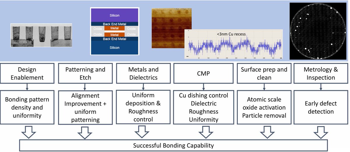
Explains that successful fine-pitch scaling shifts the focus from bonding equipment alone to total process integration.
The flow identifies six critical pillars: Design Enablement, Patterning/Etch, Metals/Dielectrics, CMP, Surface Prep, and Metrology.
Success at sub-micron levels requires atomic-scale oxide activation , precise copper dishing control (less than 3nm recess) , and early defect detection to ensure bonding capability.
3. Overlay and Alignment: The Dominant Yield Risks
Analyzes overlay tolerances, which become the primary risk factor for yield at sub-micron pitches.
At sub-micron pitch, overlay tolerances approach less than 50 nm , where any thermal drift or wafer distortion can cause catastrophic opens or shorts.
Because rework is effectively impossible after hybrid bonding and no redundancy exists at the copper-to-copper pads , misalignment leads to total die loss.
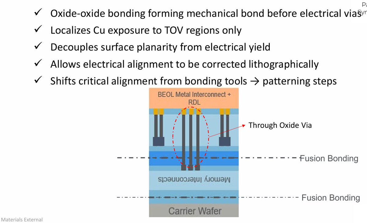
4. TOV Fusion Bonding
Introduces TOV Fusion Bonding as a complementary integration mode that bypasses the strict alignment limits of standard hybrid bonding.
This method uses oxide-to-oxide bonding to form a mechanical bond first , followed by Through Oxide Vias (TOV) to establish electrical connectivity.
By localizing copper exposure only to TOV regions , this process decouples surface planarity from electrical yield and allows for lithographic correction of electrical alignment.

As AI accelerators and data-intensive workloads accelerate the demand for tight logic-memory coupling, fine-pitch hybrid bonding has transitioned from an optional enhancement to a rigid architectural requirement. However, as interconnect scales down to sub-micron levels, process integration challenges regarding yield and alignment become paramount.
1. Packaging System Interconnect Scaling Roadmap
Visualizes the evolution of packaging interconnects and the performance gains associated with pitch scaling.
The roadmap shows a leap from Wire Bonding (less than 10 I/O per square mm, more than 10 pJ/bit) to Hybrid Bonding (10,000 to 1 million I/O per square mm, less than 0.05 pJ/bit).
Hybrid bonding reduces interconnect lengths to the micron scale , enabling ultra-high power efficiency and the future integration of Logic, Memory, and PMICs.
2. Sub-micron Fine-Pitch Scaling: From Tools to Process Integration
Explains that successful fine-pitch scaling shifts the focus from bonding equipment alone to total process integration.
The flow identifies six critical pillars: Design Enablement, Patterning/Etch, Metals/Dielectrics, CMP, Surface Prep, and Metrology.
Success at sub-micron levels requires atomic-scale oxide activation , precise copper dishing control (less than 3nm recess) , and early defect detection to ensure bonding capability.
3. Overlay and Alignment: The Dominant Yield Risks
Analyzes overlay tolerances, which become the primary risk factor for yield at sub-micron pitches.
At sub-micron pitch, overlay tolerances approach less than 50 nm , where any thermal drift or wafer distortion can cause catastrophic opens or shorts.
Because rework is effectively impossible after hybrid bonding and no redundancy exists at the copper-to-copper pads , misalignment leads to total die loss.
4. TOV Fusion Bonding
Introduces TOV Fusion Bonding as a complementary integration mode that bypasses the strict alignment limits of standard hybrid bonding.
This method uses oxide-to-oxide bonding to form a mechanical bond first , followed by Through Oxide Vias (TOV) to establish electrical connectivity.
By localizing copper exposure only to TOV regions , this process decouples surface planarity from electrical yield and allows for lithographic correction of electrical alignment.