@photon_era: Korean version will be posted ...
Korean version will be posted soon]

In the last post [PIC #1], we established that copper is struggling. At the data speeds that modern AI systems demand (hundreds of gigabits to terabits per second, across distances of meters and beyond), copper wires heat up, lose signal, and require so much circuitry just to recover that signal that the power bill becomes unsustainable.
To be more precise, there are two distinct bottlenecks. The first is between a GPU and its memory devices. This is being (partially) addressed with technologies like High Bandwidth Memory (HBM), which stacks memory dies directly on top of the GPU to dramatically shorten the electrical path. The second bottleneck that we are more interested in is longer-distance communication, such as GPU-to-GPU links. As AI clusters grow larger, GPUs spread across multiple servers and racks must constantly exchange data over distances that copper simply cannot handle at the required speeds. This is where the industry is turning to light.
But that answer immediately raises a more practical question: how? Light travels through optical fiber between cities, sure. But how do you get it onto a chip? How do you route it, control it, split it, and combine it, all within a device the size of your fingernail?
That is what this post is about. The technology is called a Photonic Integrated Circuit (PIC)— a circuit where light partially replaces electric current (the word "partially" indicates that a PIC still requires electronic integrated circuits to operate it).
The Electronic Integrated Circuit (IC) Analogy
Let's start with something more familiar: the electronic integrated circuit (IC), what people usually just call a chip. But let’s call this EIC (electronic IC) to distinguish it from photonic integrated circuit (PIC).
An EIC is a collection of electronic components, such as transistors, resistors, capacitors, metal interconnects, which are all fabricated together on a single piece of silicon. Before the EIC existed (pre-1960s), engineers built electronic circuits from individual discrete components: a transistor here, a capacitor there, all wired together by hand. The EIC changed everything by bringing all of those components onto a single substrate, dramatically reducing size, power consumption, and cost, which makes modern computing possible.
A Photonic Integrated Circuit (PIC) does the same thing, but for light.
What Does a Photonic Integrated Circuit (PIC) Look Like?

A PIC integrates optical components: lasers (which generate the light in the first place), waveguides (which is a path where light can travel like copper wires in EICs), modulators (which convert electrical signals into optical signals), photodetectors (which convert the optical signals back into electrical signals), and/or so on. Note that you do not need to know what each component does yet; it will be explained in later posts.
The most common application of PICs today is the optical transceiver. As mentioned earlier, longer-distance communication, such as GPU-to-GPU links, requires light. But GPUs speak in electrical signals. So, the electrical signal first needs to be converted into an optical signal, sent through optical fiber to the vicinity of another GPU, and then converted back into an electrical signal that the GPU can read. In short, an optical transceiver is a device that converts electrical signals from electronic hardware into optical signals or does the reverse.

For example, as shown in the image above, GPU1sends electrical signals to Optical Transceiver 1 located relatively close to the GPU. Optical Transceiver 1 converts the electrical signal into an optical signal and sends it through an optical fiber to Optical Transceiver 2 that is farther away. Finally, the received optical signal is converted back into electrical signal by Optical Transceiver 2 and sent to GPU 2.
This illustrates the fundamental concept of how light can address the data transmission bottleneck in the AI era. As the distance between devices that need to communicate each other (e.g., optical transceivers in this case) increases, light becomes significantly more advantageous than copper traces. This simple image intuitively highlights why light is so important.
However, several challenges remain. (1) Each optical component must exhibit high performance, (2) these components must be integrated onto a single chip, or at least placed close together, and (3) the entire system must be manufacturable at low cost and high volume. These are the main challenges of PIC development.
Before diving into the components of a PIC and how they work, let’s first cover some background.
The Waveguide: The Highway for Light
This is the highway through which light travels, which is the equivalent of a copper trace on a circuit board. But instead of electrons flowing through metal, photons travel through a carefully engineered structure.
Note that light exhibits both wave-like and particle-like behavior, but in this context, it is often convenient to describe it as a wave. A waveguide is a structure where light (wave) is guided along a defined path.


How does it work? You have probably heard of optical fiber, one of the key technologies that dramatically increased internet speeds over the past few decades. Optical fiber is also a highway for light to travel.
As shown in the image above, once the light enters the core (which has a higher refractive index than the cladding), it reflects at the core/cladding interface and remains confined within the core as it propagates forward. The guiding mechanism is based on total internal reflection.
Just FYI: Total internal reflection occurs when light travels from a material with a higher refractive index to one with a lower refractive index, and the incident angle is greater than the critical angle.
The loss of optical fiber is remarkably low: as low as 0.2 dB/km (95.5% of light survives after traveling 1 km) in a standard optical fiber [1]. This is the power of optical communications.
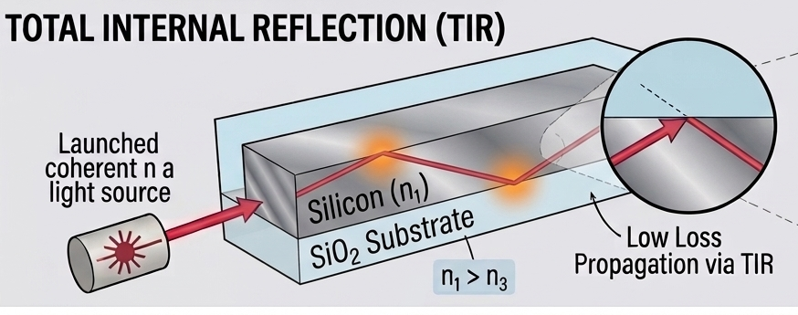
The same principle is applied to the waveguide used in photonic integrated circuits (PICs). Let’s look at the image above, which illustrates a waveguide on a PIC. A silicon with a higher refractive index is placed on a SiO2 substrate. Here, the silicon acts as the core, similar to the core in an optical fiber, while the surrounding SiO2 acts as the cladding. The refractive index n of Si in the communication wavelength range is ~ 3.5 and that of SiO2is ~1.45 [2]. Therefore, once light enters the Si, it can be confined and guided along the waveguide.
However, the loss of silicon waveguide (2~3 dB/cmin many reported cases [3]) is “much higher” than that of optical fiber (0.2~0.4 dB/km)—the units are different (dB/cm vs. dB/km). This is mainly due to two reasons: (1) the sidewall roughness introduced during the etching process causes scattering loss; and (2) silicon has higher optical absorption than SiO2, which is the core material of an optical fiber (the core material of optical fiber is SiO2). We will discuss this further in later posts. For now, the key point is the basic concept of the waveguide.
Why Silicon?
You might ask: Why are PICs fabricated specifically on silicon? There are other materials that can be used to build waveguides and photonic circuits, so why has silicon emerged as the dominant platform?
There are three main reasons, and they all come down to manufacturing advantages as well as cost.
Reason 1: CMOS Compatibility (Compatible with Existing Infrastructure)
Silicon photonic devices can be fabricated using the same equipment and processes as standard CMOS microelectronics, which is the same technology behind every CPU, GPU, and memory chip in existence (note that CMOS is a well-known widely adopted electronic component). This means silicon photonic circuits can be made in advanced semiconductor fabs such as GlobalFoundries, TSMC, Intel. Instead of building a separate and exotic manufacturing infrastructure from scratch, silicon photonics can leverage one of the most sophisticated high-volume manufacturing systems ever created.
Reason 2: Wafer-Scale Manufacturing
Silicon is one of the most abundant elements on Earth, and silicon-on-insulator (SOI) wafer technology has been established very well (as large as 12 inches or 300 mm in diameter), yielding hundreds to thousands of chips per wafer.
In contrast, III-V semiconductor materials such as indium phosphide (InP), which are used for some photonic functions (especially lasers), are typically grown on much smaller wafers, about 3 to 4 inches in diameter (~75 to 100 mm), and cost far more per unit area.
As a result, silicon can dramatically reduce the cost per chip compared with III-V-only approaches.
Reason 3: Co-Integration with Electronics
Even though light replaces some electronic interconnects, optical components still require electronics to operate. Because silicon photonics is compatible with semiconductor manufacturing, photonic devices can be integrated on the same package, or in some cases alongside the same die stack, as the electronics that control them. This can reduce cost, power consumption, and parasitic losses. More importantly, this proximity becomes especially important at very high speeds. At bandwidth of 100 GHz and beyond, even short electrical interconnects can introduce significant problems such as loss, heat, power consumption and so on.
Unfortunately, nothing is perfect. Silicon also has important limitations.
The Integration Challenge: Why This Is Hard
In EICs (electronic integrated circuits), most key components (e.g., transistors, capacitors, resistors, and metal interconnects) are built using a relatively small set of materials: silicon, silicon dioxide, and metals. More importantly, they are fabricated through highly standardized process flows on the same wafer. You pattern one layer, deposit the next, etch, repeat. Every component comes out of that same process. This manufacturing model is one reason electronic chips have become so inexpensive, dense, and scalable.
Photonics is different. No single material performs every optical function well.
1. Light sources
A light source is essential in silicon photonics system. However, silicon is not suitable for light emission due to its indirect bandgap, and thus, III-V semiconductor materials such as InP or GaAs are commonly used for lasers.
2.Photodetectors
To convert optical signals back into electrical signals, high-speed photodetectors are required. Unfortunately, intrinsic silicon has limited absorption at telecommunication wavelengths (e.g., 1310 and 1550 nm), making it suboptimal for many detector designs. Materials like germanium (Ge) are widely integrated for photodetection [4].
3. Modulators
A modulator converts electrical signals into optical signals. Silicon can be used for modulators, but its electro-optic response is weaker than some alternative materials. For very high-speed or low-voltage operation, materials like lithium niobate can offer significant advantages in bandwidth and drive voltage [5].
All of this means that high-performance PICs often require materials beyond silicon to be integrated onto a silicon platform. Bringing multiple materials together on the same chip—or at least within the same package—is known as heterogeneous integration. Architectures such as co-packaged optics (CPO) are one example. This is one of the central engineering challenges in modern photonics, and we will discuss it in later posts.
This is not a problem without solutions but a problem with several competing solutions. The industry is actively determining which approaches scale best in cost, yield, reliability, and volume production. The fact that companies such as Intel, Marvell, Broadcom, and Coherent have shipped silicon photonics products at large scale shows that many of these integration challenges are already being addressed. The next question is how to do it better, cheaper, and at higher volume.
Summary and What’s Next?
In this post, we built a basic understanding of what a photonic integrated circuit (PIC) is and why silicon has become the dominant platform.
As GPUs increasingly need to communicate with one another, high-speed data transmission between chips becomes critical. Conventional copper traces (electrical interconnects) are approaching their limits as transmission distances increase and data rates continue to rise. Their main challenges are heat generation, limited bandwidth (speed), and high power-consumption.
Optical signals can travel much longer distances with far lower loss than electrical signals in copper. We already know this from optical fiber, which has been commercially deployed for decades and connects devices across cities, countries, and continents.
This is why optical transceivers have attracted so much attention: they convert electrical signals into optical signals, send them through optical fibers, and then convert them back into electrical signals at the destination.
Silicon has become the leading platform for optical transceivers for three key reasons: CMOS compatibility, wafer-scale manufacturing, and close integration with electronics.
However, challenges remain. No single material performs every optical function well, which means materials beyond silicon often need to be integrated onto the same chip—or at least packaged nearby. Solving this efficiently is one of the central challenges of the industry. We will discuss this in this series.
In the next chapter, we will explore how PICs actually work, with a focus on grating couplers.
Side Note – Corning, an Optical Fiber Company

Let’s pause here and shift slightly.
This figure above gives us one additional insight. We have discussed the importance of optical transceivers, but what connects them isoptical fiber, a technology that has been commercially mature for decades. As the optical transceiver market grows, demand for optical fiber grows with it. And the numbers are striking. Demand for optical fiber in AI applications grew by 138% year-on-year in 2024, and generative AI datacenters are expected to require more than 10 times as much optical fiber as traditional data center networks [6].
Corning Inc. is the world's leading optical fiber manufacturer and is perhaps one of the clearest illustrations of this trend. The company reported $6.3 billion in optical communications revenue in 2025, up 35% year-over-year, with enterprise data center revenue growing 61% [7]. In January 2026, Meta signed a $6 billion contract with Corning to supply optical fiber for new AI data centers [8]. It is therefore not surprising that Corning's stock (NYSE: GLW) has risen over 200% in the past 1 year.
📷
Though this post is not intended as investment advice, I would like to share a few thoughts.
On the positive side:
(1) Demand for optical fiber is structurally tied to AI datacenter growth, and thus, as more GPUs are connected, more fiber is needed.
(2)Corning is, to my knowledge, one of the few globally scaled US-based manufacturers that produces the glass fiber itself, which may be strategically valuable as major AI infrastructure spending is led by US-based hyperscalers such as Microsoft, Meta, and Amazon.
On the other hand:
(3) Roughly 33% of Corning's revenue comes from display glass and specialty materials, meaning the stock is not a pure-play on fiber demand [7].
(4) Strong competitors exist outside the US, including Prysmian (Italy) and YOFC (China).
References
[1] T. Miya et al., "Ultimate low-loss single-mode fibre at 1.55 μm," Electronics Letters15, 106 (1979). [DOI: 10.1049/el:19790077]
[2] B. Jalali et al., “Silicon Photonics,” Journal of Lightwave Technology24, 4600 (2006). [DOI: 10.1109/JLT.2006.885782]
[3] S. Shekhar et al., “Roadmapping the next generation of silicon photonics,” Nature Communications15, 751 (2024). [DOI: 10.1038/s41467-024-44750-0]
[4] J. Michel et al., “High-performance Ge-on-Si photodetectors,” Nature Photonics4, 527–534 (2010). [DOI: 10.1038/nphoton.2010.157]
[5] C. Wang et al. "Integrated lithium niobate electro-optic modulators operating at CMOS-compatible voltages." Nature562, 101-104 (2018). [DOI: 10.1038/s41586-018-0551-y]
[6] CJ Staff, “Meta-Corning deal puts NC at center of AI infrastructure push,” Carolina Journal (January 27, 2026). https://www.carolinajournal.com/meta-corning-deal-puts-nc-at-center-of-ai-infrastructure-push/
[7] Corning Incorporated, “Corning Announces Outstanding 2025 Financial Results,” Investor Relations Press Release (January 28, 2026). https://investor.corning.com/news-and-events/news/news-details/2026/Corning-Announces-Outstanding-2025-Financial-Results-1--Upgrades-Springboard-Plan-for-Faster-Sales-Growth-on-Significantly-Enhanced-Financial-Profile/default.aspx
[8] K. Tarasov, “Meta inks deal to pay Corning up to $6 billion for fiber-optic cables,” CNBC (January 27, 2026). https://www.cnbc.com/2026/01/27/apple-supplier-corning-wins-6-billion-from-meta-for-ai-optical-fiber.html